Guangzhou Yueshi Semiconductor Project: JB Spring Vibration Isolator Contract
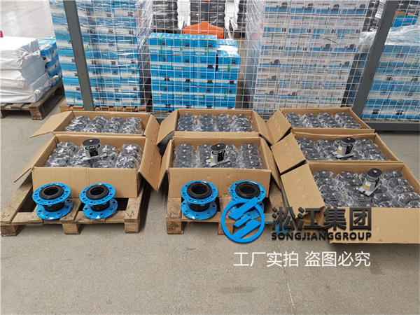
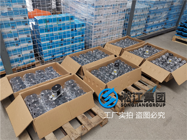
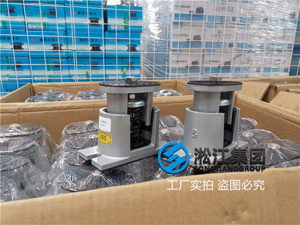
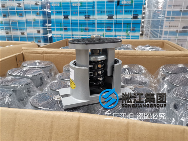
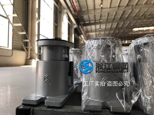
Shanghai Songjiang Shock Absorber Group Co., Ltd.’s official website presents: Contract information for JB Spring Vibration Isolators for the Guangzhou Yueshi Semiconductor Project. Songjiang Group provides noise reduction solutions for the air conditioning systems of numerous semiconductor projects in China, along with supplying high-quality spring vibration isolators.
![]()
![]()
![]()
Introduction to Guangzhou Yueshi Semiconductor Project:
The Yueshi 12-inch wafer project was launched in the Huangpu District, Guangzhou Development Zone. With a total investment of 28.8 billion yuan, it is the first and only 12-inch chip production line in Guangzhou and Guangdong Province.
Yueshi Semiconductor has been listed as a key construction project in Guangdong Province and Guangzhou Municipality. The project has a total investment of 28.8 billion yuan and is divided into two phases.
Chips are regarded as the “industrial grain” and are the “heart” of complete equipment. In 2018, China’s total chip imports amounted to $312 billion, accounting for nearly 60% of the global integrated circuit market size of $500 billion. Chip imports exceeded that of oil, ranking first among imported goods in China. “Chip localization” has become a long-term important development strategy for the country.
Guangzhou Yueshi Semiconductor Technology Co., Ltd. (referred to as “Yueshi Semiconductor”) is the first 12-inch chip factory in China to operate with a Virtual IDM (Virtual IDM) strategy. It has been listed as a key construction project in Guangdong Province and Guangzhou Municipality. The project has a total investment of 28.8 billion yuan, divided into two phases. The first phase of investment is 10 billion yuan, focusing on the manufacturing of 0.18um-90nm analog chips and discrete devices, achieving a production capacity of 40,000 12-inch wafers per month. The second phase of investment is 18.8 billion yuan, focusing on the world’s most advanced high-end 65nm-40nm high-voltage BCD analog chip technology, with a production capacity of 40,000 12-inch wafers per month.
Regarding production technology, Li Haiming, Vice President of Yueshi Semiconductor Technology Co., Ltd., introduced that 12-inch wafer chips are currently the main technical products of multinational companies. Chinese manufacturers mainly produce 6-inch and 8-inch wafers, and the self-sufficiency rate of 12-inch wafer chips is very low. The larger the wafer size, the more chips can be produced on the same wafer, which can greatly reduce product costs, but also requires higher material and production technology. Compared with the 8-inch wafer production line, the efficiency of Yueshi’s 12-inch wafer production line can reach 2.25 times.
The project is positioned for differentiated, customized operations, focusing on high-end analog chips, automotive electronics, biomedicine testing, 5G front-end modules, and other domestically scarce products. It is expected to achieve sales targets of tens of billions and further drive the formation of a trillion-level output value scale for upstream and downstream enterprises.
On the day the Yueshi 12-inch wafer project was put into production, Yueshi Semiconductor signed contracts with more than 20 semiconductor industry-academia-research units such as the Institute of Microelectronics of the Chinese Academy of Sciences, the School of Microelectronics of Sun Yat-sen University, the School of Microelectronics of South China University of Technology, the School of Microelectronics of Fudan University, Guangzhou Anbao Electronics Co., Ltd., and Geek Microelectronics (Shanghai) Co., Ltd., to jointly carry out industry-academia-research cooperation and jointly cultivate talents for the development of the semiconductor industry.
By 2022, Huangpu will become a national integrated circuit industry agglomeration area. At the end of 2018, the “Measures for Accelerating the Development of the Integrated Circuit Industry in Guangzhou” proposed that Guangzhou, with Huangpu District and Guangzhou Development Zone as the core, plans to implement seven major projects covering chip manufacturing enhancement, chip design improvement, packaging and testing chain strengthening, supporting industry supplementation, innovation capability breakthroughs, coordinated industry development, and talent introduction and cultivation, striving to build a national integrated circuit industry agglomeration area, talent gathering place, and innovation demonstration zone by 2022.
The Yueshi 12-inch wafer project pioneered the Virtual IDM (Virtual IDM) operating mode in China. It is reported that Yueshi Semiconductor is responsible for the construction and operation of the 12-inch chip factory, and jointly customizes the development of process platforms with chip design customers, seamlessly connecting “chip design”, “manufacturing”, and “customer market application requirements”.
Since the start of construction of Yueshi Semiconductor, 80 integrated circuit industry chain companies have come to visit, and 32 companies have registered and settled, with over 7 companies achieving annual turnover of over 100 million yuan. These projects cover various fields such as design, packaging and testing, equipment, and materials in the upstream and downstream industries, forming a complete industrial chain ecosystem with Yueshi Semiconductor as the leader, integrating “chip design-manufacturing-packaging testing-terminal application”. With more and more semiconductor companies gathering, Huangpu plans to build a new energy and new material value innovation park in the Knowledge City where the Yueshi project is located. The planned area of the park is 6.4 square kilometers, with the Integrated Circuit Industry Innovation Park as the “park within the park”, focusing on core companies such as the Yueshi project, introducing a batch of large-size wafer production line projects, striving for significant progress in fields such as compound semiconductor devices, microelectromechanical systems, power semiconductor devices, characteristic processes, and third-generation semiconductor materials; comprehensively entering the fields of computing, storage, and mobile communication chips, introducing a batch of well-known domestic and foreign companies in the new material field, forming a relatively complete industrial chain, and building it into a Guangzhou Intellectual Manufacturing Park.
![]()
Related link:SHA-S-60 Horizontal Volute Pump Side Support Spring Vibration Isolators


